 INNO fibre optic temperature sensors ,temperature monitoring systems.
- Precise wafer temperature measurement is critical in semiconductor manufacturing, affecting yield rates by up to 35% in advanced processes.
- The silicon wafer temperature range must be controlled within ±0.5°C during critical processes to ensure consistent product quality.
- Fiber optic sensors enable non-intrusive, accurate wafer surface temperature measurement without introducing electromagnetic interference.
- Thermal monitoring solutions now include wireless temperature wafer systems capable of real-time, in-situ measurements during actual production.
- Advanced temperature sensing wafer technologies can measure temperature distributions across 300mm wafers with spatial resolution below 1mm.
Understanding Wafer Temperature Challenges in Semiconductor Manufacturing
Temperature uniformity across semiconductor wafers is one of the most critical parameters in modern fabrication processes. Even minor temperature variations can significantly impact product quality, reliability, and manufacturing yield. With transistor dimensions now measured in nanometers, thermal control requirements have become increasingly stringent.
The challenges of wafer temperature measurement are multifaceted. The semiconductor processing environment presents unique constraints including vacuum conditions, reactive chemistries, high electromagnetic fields, and the need for non-contact methods that won’t contaminate the wafer. Additionally, modern processes require real-time data across the entire wafer surface rather than at discrete points.
Temperature-related issues can manifest in numerous ways throughout the semiconductor manufacturing process:
- Film thickness variations during deposition
- Uneven etching profiles and rates
- Inconsistent dopant activation during annealing
- Photoresist development variations
- Stress-induced wafer warping
- Unpredictable chemical reaction rates
Industry data suggests that temperature non-uniformities account for approximately 22% of yield losses in advanced semiconductor processes, making thermal monitoring one of the highest-value improvement opportunities in modern fabs.
Critical Temperature Parameters and Requirements
Different semiconductor processes have specific wafer temperature requirements:
| Process | Typical Temperature Range | Uniformity Requirement | Temporal Stability |
|---|---|---|---|
| Photolithography | 20-25°C | ±0.1°C | ±0.05°C/min |
| Chemical Vapor Deposition | 300-800°C | ±2.0°C | ±0.5°C/min |
| Rapid Thermal Annealing | 900-1100°C | ±3.0°C | ±5.0°C/sec (ramp) |
| Ion Implantation | -20 to 100°C | ±1.0°C | ±0.2°C/min |
| Plasma Etching | -20 to 150°C | ±1.0°C | ±0.3°C/min |
| Wafer Bonding | 200-450°C | ±2.0°C | ±1.0°C/min |
| Wafer Testing | -55 to 125°C | ±0.5°C | ±0.1°C/min |
The silicon wafer temperature range for processing spans from cryogenic temperatures to over 1100°C, approaching the silicon wafer melting temperature of 1414°C. This extremely wide range presents significant measurement challenges, as no single temperature sensing technology works optimally across all conditions.
Expert Insight:
The silicon wafer maximum temperature for processing is typically limited to around 1200°C in production environments, providing a safety margin below the melting point. However, even at temperatures well below this limit, thermal-induced stresses can cause wafer warping and defect generation if temperature gradients exceed critical thresholds.
Traditional Wafer Temperature Measurement Approaches
Conventional methods for measuring wafer temperature include:
Thermocouples
- Operation: Uses the thermoelectric effect to generate voltage proportional to temperature difference
- Advantages: Low cost, wide temperature range, proven technology
- Limitations: Contact-based, potential contamination source, point measurement only, susceptible to EMI
- Applications: Wafer chuck temperature control, equipment qualification, non-production monitoring
Resistance Temperature Detectors (RTDs)
- Operation: Measures temperature-dependent change in electrical resistance
- Advantages: Higher accuracy than thermocouples, good stability
- Limitations: Contact-based, limited high-temperature range, requires excitation current
- Applications: Precise wafer substrate temperature control in low-temperature processes
Pyrometry (IR Thermometry)
- Operation: Non-contact measurement of infrared radiation emitted by the wafer
- Advantages: Non-contact, suitable for high temperatures, rapid response
- Limitations: Emissivity-dependent, affected by background radiation, limited low-temperature capability
- Applications: Rapid thermal processing, silicon wafer annealing temperature monitoring
Integrated Test Wafers
- Operation: Special wafers with embedded temperature sensors that mimic product wafers
- Advantages: Measures actual conditions experienced by production wafers
- Limitations: Not used during actual production, limited durability, expensive
- Applications: Process development, tool qualification, wafer testing over multiple temperatures
While these methods have served the industry for decades, the increasing precision requirements of advanced semiconductor processes have exposed their limitations. Modern manufacturing demands non-contact, whole-wafer temperature monitoring with higher accuracy than traditional approaches can provide.
Advanced Wafer Temperature Sensor Technologies
Several breakthrough technologies have emerged to address the limitations of traditional temperature monitoring methods:
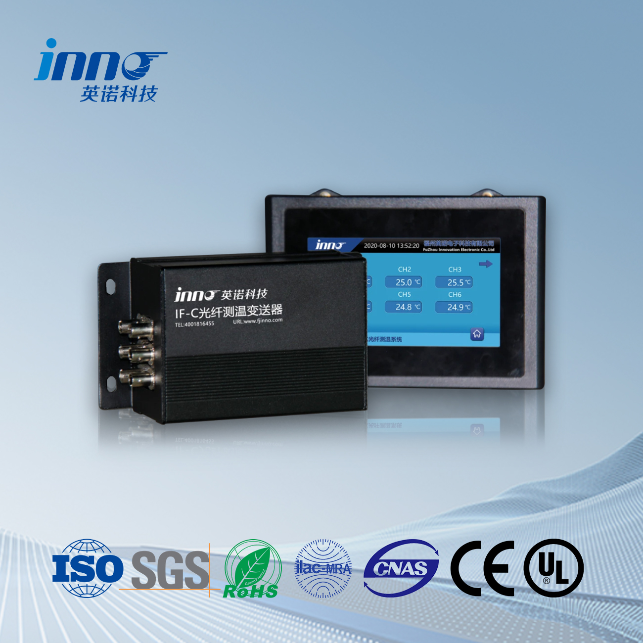
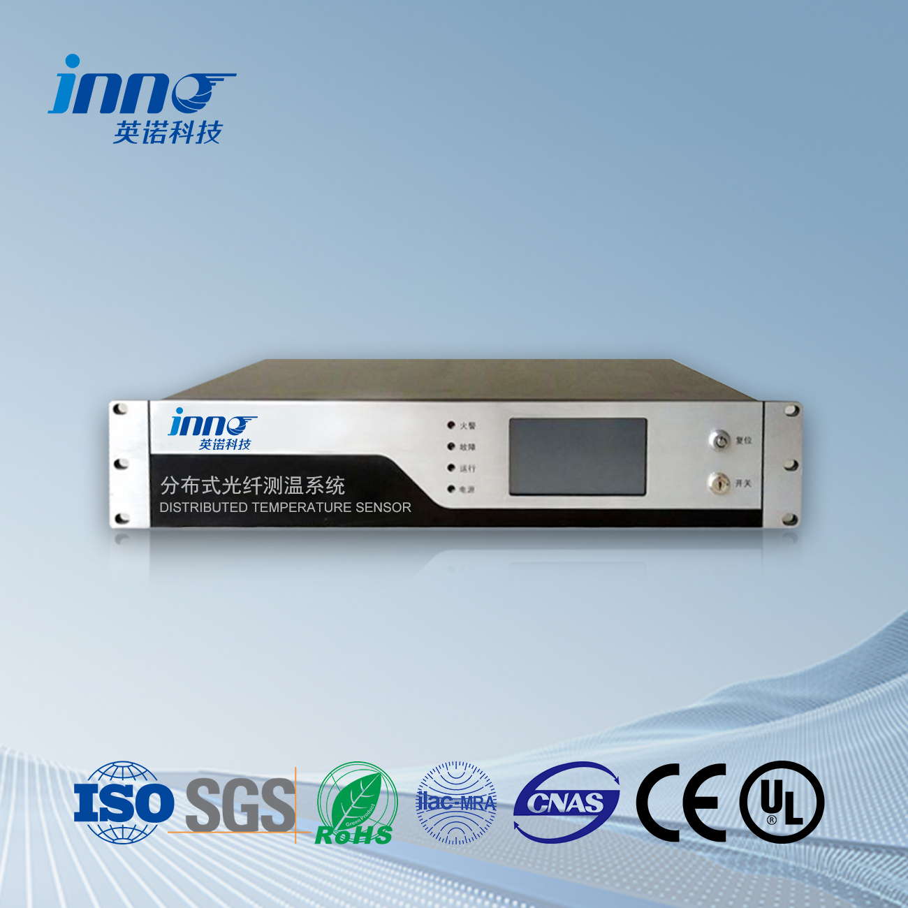
Fiber Optic Temperature Sensing Solutions
Fiber optic sensors represent one of the most promising technologies for advanced wafer surface temperature measurement:
- Operation: Uses temperature-dependent optical properties of specially designed fiber tips or coatings
- Advantages:
- Completely immune to electromagnetic interference
- No electrical connections (intrinsically safe)
- Extremely small size enables minimal thermal mass
- Compatible with harsh processing environments
- Capable of distributed sensing along fiber length
- Wide temperature range capability (-269°C to +1200°C with appropriate fibers)
- Implementations:
- Fluoroptic Sensors: Uses temperature-dependent fluorescent decay times
- Fiber Bragg Grating: Measures temperature-induced shifts in reflected wavelength
- Distributed Temperature Sensing: Measures backscattered light along entire fiber
- Applications: In-situ wafer temperature measurement, silicon wafer temperature measurement, high-precision thermal profiling
Industry Application: High-Precision Fiber Optic Monitoring
A leading semiconductor manufacturer implemented fiber optic temperature sensors for monitoring silicon wafer temperature during critical etching processes. The system achieved ±0.1°C accuracy across 300mm wafers, allowing the company to reduce temperature-related defects by 62% and increase yield by 3.8% for their most advanced process node, representing annual savings of $4.2 million for a single production line.
Wireless Temperature Wafer Systems
Wireless monitoring systems represent a revolutionary approach to wafer temperature measurement:
- Operation: Battery-powered sensors embedded in wafer-like carriers transmit real-time temperature data during actual processing
- Advantages:
- Measures actual conditions experienced by production wafers
- Real-time data during actual processing steps
- Multiple sensors provide thermal mapping across entire wafer
- Can traverse entire process flow for comprehensive analysis
- No external connections or wires required
- Limitations:
- Not suitable for extremely high-temperature processes
- Limited battery life
- Higher cost than conventional sensors
- Not used during actual production
- Applications: Wafer temperature measurement wireless solutions for process development, tool qualification, troubleshooting
The SensArray wafer temperature monitoring system is a prominent example of this technology, providing up to 65 measurement points across a single wafer carrier. These systems have become invaluable tools for process engineers seeking to optimize thermal uniformity.
Thin-Film Temperature Sensors
Advanced semiconductor processes can now incorporate temperature sensors directly onto test wafers:
- Operation: Thin-film resistive temperature devices fabricated directly on silicon wafers
- Advantages:
- Minimal thermal mass
- Direct measurement at wafer surface
- Can be integrated into production-like wafers
- Multiple sensors provide detailed thermal mapping
- Limitations:
- Complex fabrication process
- Limited high-temperature operation
- Requires specialized data acquisition systems
- Applications: Wafer temperature stress simulation, wafer level trimming in temperature sensor manufacturing, process optimization
Multi-Wavelength Pyrometry
Advancements in pyrometry have addressed many limitations of traditional IR measurement:
- Operation: Measures thermal radiation at multiple wavelengths to compensate for emissivity variations
- Advantages:
- Non-contact measurement
- Reduced sensitivity to emissivity variations
- Suitable for high-temperature processes
- Real-time measurement capability
- Limitations:
- Complex calibration requirements
- Still affected by chamber window contamination
- Limited applicability at lower temperatures
- Applications: Silicon wafer max temperature monitoring, rapid thermal processing, annealing processes
Specialized Applications in Wafer Temperature Monitoring
Several specific semiconductor manufacturing processes present unique thermal monitoring challenges:
Low Temperature Wafer Bonding
Wafer bonding processes are particularly sensitive to thermal conditions:
- Process Description: Joining of two wafer surfaces via atomic bonds, often used for 3D integration and MEMS fabrication
- Temperature Challenges:
- Uniform pressure application during temperature ramps
- Thermal expansion coefficient mismatches between materials
- Precise control of direct wafer bonding temperature
- Managing stress during cooling phases
- Monitoring Solutions:
- Distributed fiber optic sensors for spatial temperature mapping
- Specialized temperature sensing wafer carriers with multiple measurement points
- In-situ infrared imaging through specialized viewports
- Critical Parameters: Hydrophilic low-temperature direct wafer bonding typically requires ±1.0°C uniformity during critical bond formation stages
Application Note:
For low temperature glass to glass wafer bonding, fiber optic sensors are particularly valuable due to their ability to provide precise measurements in the 200-400°C range without introducing electromagnetic interference that could affect the electrostatic bonding process. Recent advancements have enabled successful bonding at temperatures as low as 180°C while maintaining bond strengths above 15 MPa.
Silicon Wafer Thermal Expansion Coefficient at Various Temperatures Considerations
Thermal expansion introduces significant challenges in many processes:
- Physical Principle: Silicon expands non-linearly with temperature, with the coefficient of thermal expansion (CTE) itself varying with temperature
- Manufacturing Impact:
- Pattern misalignment between process layers
- Wafer warping during non-uniform heating/cooling
- Aluminum film stress with temperature on si wafer causing reliability issues
- Critical dimension variations across the wafer
- Monitoring Requirements:
- High spatial resolution temperature mapping
- Correlation of temperature profiles with physical distortion
- Real-time feedback for dynamic temperature control
- Technical Solution: Wafer temperature stress simulation combined with real-time monitoring enables predictive compensation for thermal expansion effects
Understanding and controlling silicon wafer temperature shrinkage effects is particularly critical in processes with multiple high-temperature steps, as cumulative stress can lead to wafer breakage or yield loss.
Semiconductor Wafer Storage Temperature Monitoring
Even during storage, temperature control remains important:
- Storage Requirements:
- Typical storage range: 20-25°C for most wafers
- Humidity control: 35-55% relative humidity
- Temperature stability: ±2°C maximum variation
- Gradual temperature changes only (≤0.5°C/min)
- Temperature-Related Risks:
- Moisture absorption affecting subsequent processing
- Photoresist degradation on coated wafers
- Oxidation rate changes affecting surface properties
- Metal contamination diffusion activation
- Monitoring Approach: Environmental monitoring systems with multiple temperature and humidity sensors, often fiber-optic based to eliminate electromagnetic interference
Silicon Wafer Oxide Temperature Control
Thermal oxidation processes require precise temperature monitoring:
- Process Description: Controlled growth of silicon dioxide layers through reaction with oxygen at elevated temperatures
- Temperature Considerations:
- Growth rate varies exponentially with temperature (±1°C = ±5% thickness variation)
- Temperature uniformity directly affects oxide thickness uniformity
- Ramp rates affect oxide quality and stress
- Monitoring Solutions:
- Multi-point fiber optic temperature sensors within oxidation furnace
- Specialized thermocouples with appropriate sheathing for oxidizing atmospheres
- Test wafers with embedded sensors for qualification runs
Low Temperature Wafer Probing
Testing semiconductors across temperature ranges requires specialized monitoring:
- Process Description: Electrical testing of devices at various temperatures to characterize performance
- Temperature Challenges:
- Maintaining stable temperatures during extended test sequences
- Thermal cycling effects on probe contacts
- Condensation prevention during below-ambient testing
- Managing silicon wafer resistivity at low temperature changes
- Monitoring Solutions:
- Integrated RTD sensors in test chucks
- Non-contact IR thermometry for spot checks
- Specialized test wafers with temperature sensors for system calibration
Understanding how silicon wafer resistivity calculation temperature dependencies affect measurement is crucial for accurate device characterization across operating temperature ranges.
Implementing Advanced Wafer Temperature Measurement Systems
Successfully deploying advanced thermal monitoring requires careful planning and implementation:
System Selection Considerations
- Process Requirements Analysis
- Temperature range required (min/max)
- Required measurement accuracy and resolution
- Spatial coverage needs (point measurement vs. mapping)
- Temporal requirements (sampling rate, response time)
- Environment compatibility (vacuum, chemicals, plasma, etc.)
- Technology Selection
- Fiber optic for EMI immunity and high-temperature applications
- Wireless systems for comprehensive process characterization
- Thin-film RTDs for precise surface measurements
- Multi-wavelength pyrometry for high-temperature non-contact needs
- Integration Requirements
- Data collection and storage infrastructure
- Process control system integration
- Analysis software capabilities
- Retrofit capabilities for existing equipment
Implementation Best Practices
- Calibration Strategy
- Regular calibration schedule based on application criticality
- On-site calibration capabilities where possible
- Multiple reference standards for cross-verification
- Temperature cycling during calibration to verify dynamic response
- Deployment Approach
- Phased implementation starting with most critical processes
- Baseline current performance before new system deployment
- Parallel monitoring during transition periods
- Comprehensive validation protocol development
- Personnel Training
- Operator training on system operation and limitations
- Engineering staff training on data interpretation
- Maintenance procedures and troubleshooting protocols
- Regular knowledge refreshers and updates on system enhancements
Data Integration and Analysis
Maximizing the value of temperature data requires sophisticated analysis approaches:
- Real-time Monitoring
- Live temperature maps displaying spatial distribution
- Automated alarm systems for deviation from specifications
- Process control feedback for dynamic adjustment
- Historical Analysis
- Trend analysis for slow-developing issues
- Correlation of temperature data with yield metrics
- Comparative analysis between tools and chambers
- Process capability studies for optimization
- Advanced Analytics
- Machine learning algorithms for pattern recognition
- Predictive maintenance based on thermal signatures
- Digital twin modeling for process optimization
- Statistical process control implementation
Implementation Insight:
Advanced fabs are now implementing integrated data platforms that combine wafer temperature measurement data with other process parameters and metrology results, enabling AI-driven analytics that can identify complex multi-variable interactions affecting yield. These systems have successfully identified subtle thermal signature patterns that precede equipment failures by weeks or months.
Case Studies in Advanced Wafer Temperature Monitoring
Case Study 1: Etching Process Optimization with Fiber Optic Sensing
A leading semiconductor manufacturer investigated yield issues in their advanced node etch process:
- Challenge: Unexplained critical dimension (CD) variations across wafers and between batches in a plasma etching process
- Investigation: Analysis revealed the question “does wafer temperature effect etch rate?” was central to the issue
- Implementation: Deployed fiber optic wafer surface temperature measurement system with 17 measurement points across 300mm wafers
- Findings: Discovered non-uniform cooling gas distribution creating temperature variations of 4.3°C across wafers
- Resolution: Redesigned gas distribution system and implemented real-time temperature feedback control
- Results: CD uniformity improved by 42%, associated yield increase of 7.2%, representing $11.4M annual savings
Case Study 2: Room Temperature Direct Wafer Bonding Enhancement
A MEMS manufacturer struggled with bond strength and yield in a room-temperature bonding process:
- Challenge: Inconsistent bond strength and high void density in surface-activated direct bonding process
- Investigation: Used temperature sensing wafer to discover micro-scale temperature non-uniformities during plasma activation
- Implementation: Integrated fiber optic sensors to provide real-time monitoring during the activation process
- Modification: Revised the process to use controlled, ultra-low temperature (50°C) annealing with precise thermal mapping
- Results: Void density reduced by 78%, bond strength increased by 40%, overall yield improvement of 31%
This case demonstrated that even processes labeled as “room temperature direct wafer bonding” benefit from precise thermal mapping and minor thermal optimization.
Case Study 3: Multi-Temperature Testing Optimization
A semiconductor manufacturer faced challenges with final test yields across temperature ranges:
- Challenge: High failure rates during wafer testing over multiple temperatures, particularly at temperature transitions
- Investigation: Deployed wireless temperature wafer system to monitor actual die temperatures during test sequences
- Discovery: Significant lag between chuck temperature and actual die temperature, plus non-uniform heating/cooling across wafer
- Implementation: Revised test soak times based on actual measured thermal response, modified test chuck design
- Results: Test time reduced by 18% while improving correlation between wafer-level and final package testing by 23%
Future Trends in Wafer Temperature Monitoring
The field of semiconductor thermal monitoring continues to evolve rapidly with several emerging trends:
Integrated Multi-Parameter Sensing
Next-generation monitoring will combine temperature with other parameters:
- Combined temperature and stress sensors in single packages
- Integration of temperature and vibration monitoring
- Multi-parameter wafer surface temperature measurement systems
- Correlation of temperature with real-time process gases analysis
Advanced Materials and Sensor Designs
New materials are enabling enhanced sensor capabilities:
- Graphene-based ultra-thin thermal sensors
- Quantum dot temperature sensing for nanoscale resolution
- Phase-change material sensors for specific temperature thresholds
- Self-powered thermal sensors using thermoelectric effects
AI and Machine Learning Integration
Artificial intelligence is transforming data analysis:
- Predictive thermal modeling based on historical process data
- Real-time anomaly detection in thermal patterns
- Automated process optimization through thermal feedback
- Digital twin models incorporating comprehensive thermal behavior
Advanced Integration Technologies
Emerging techniques will further enhance monitoring capabilities:
- Temperature-sensing films integrated directly into production wafers
- Embedded temperature monitoring in key process consumables
- Continuous manufacturing lines with integrated thermal mapping
- Cross-platform data standardization for comprehensive analysis
Frequently Asked Questions About Wafer Temperature Measurement
What is the primary advantage of fiber optic sensors for wafer temperature measurement?
Fiber optic sensors offer complete immunity to electromagnetic interference, which is critical in semiconductor processing environments with RF plasma, high magnetic fields, and other electromagnetic noise sources. Additionally, they provide no ignition source, introduce no metallic contaminants, can withstand extreme temperatures, and can be made extremely small with minimal thermal mass that won’t affect the measurement itself.
How does wafer temperature affect photoresist processing?
Temperature significantly impacts photoresist processing in multiple ways. When spinning photoresist on wafer with different temperatures, viscosity changes can cause thickness variations. During baking, temperature uniformity directly affects solvent evaporation rates and resultant film properties. Even small temperature variations (±1°C) can impact critical dimension control, sidewall profiles, and adhesion properties, particularly for advanced nodes with tight process windows.
Does wafer temperature effect wet etch rate?
Yes, wafer temperature significantly affects wet etch rates, typically following an Arrhenius relationship where each 10°C increase results in approximately 1.5-2.5× faster etch rate (depending on the specific chemistry). This temperature sensitivity makes precise thermal control critical for wet processes. Even localized temperature variations across a wafer can result in non-uniform material removal, affecting feature dimensions and potentially causing yield loss.
How are point defects in silicon wafer temperature related?
Temperature plays a crucial role in point defect dynamics in silicon. At elevated temperatures, vacancy and interstitial concentrations increase exponentially, affecting defect formation, migration, and annihilation rates. Thermal processing history directly impacts the concentration of grown-in defects. Rapid temperature changes can freeze in non-equilibrium defect concentrations. Advanced wafer temperature measurement systems help optimize thermal processes to minimize detrimental defect formation while enhancing beneficial defect engineering.
What temperature range is used for silicon wafer annealing temperature processes?
Silicon wafer annealing temperatures vary widely depending on the specific purpose. Dopant activation typically requires 900-1050°C, while stress relief annealing might use 600-800°C. Hydrogen annealing for surface preparation often runs at 800-1100°C. Advanced flash and laser annealing can reach surface temperatures of 1200-1300°C for milliseconds or microseconds. The precise control of these temperatures, including ramp rates and uniformity, is critical for desired electrical and material properties.
Conclusion: The Critical Importance of Advanced Wafer Temperature Monitoring
As semiconductor manufacturing advances toward smaller geometries, more complex structures, and larger wafer sizes, the importance of precise wafer temperature measurement continues to grow. Temperature variations that were once negligible now have significant impacts on product quality, reliability, and manufacturing yield.
Fiber optic sensing technologies have emerged as the premier solution for advanced thermal monitoring, offering unique advantages in accuracy, immunity to interference, and compatibility with harsh processing environments. These systems enable semiconductor manufacturers to achieve unprecedented temperature control, directly translating to improved yields, enhanced product quality, and accelerated process development.
The integration of advanced analytics with comprehensive thermal data is transforming semiconductor manufacturing, enabling predictive process control and optimization that were previously impossible. As the industry continues to push the boundaries of semiconductor technology, advanced wafer temperature monitoring will remain a critical enabler of future innovations.
Manufacturers who implement comprehensive thermal monitoring strategies position themselves for superior yields, faster problem resolution, and ultimately improved competitive advantage in this highly demanding industry.

Fiber optic temperature sensor, Intelligent monitoring system, Distributed fiber optic manufacturer in China
 |
 |
 |