 INNO glasvezel temperatuursensoren ,temperatuurbewakingssystemen.
- Bewaking van de temperatuur van halfgeleiders is de praktijk van het meten en regelen van temperaturen op waferniveau, binnen proceskamers, en tussen subsystemen van apparatuur om de herhaalbaarheid van processen te garanderen, maximaliseer de opbrengst, en bescherm gevoelige componenten.
- Fluorescerende glasvezeltemperatuursensoren zijn bij uitstek geschikt voor halfgeleideromgevingen omdat ze immuun zijn voor elektromagnetische interferentie, RF-velden, en plasma-energie – allemaal gebruikelijk in productieprocessen.
- Kritische monitoringpunten zijn onder meer CVD-kamers, etsreactoren, diffusion furnaces, PVD-sputtersystemen, lithografische stadia, CMP plaatreiniger, en waferhouders.
- Glasvezelsensoren introduceren geen metaalverontreiniging, voldoen aan strenge normen voor cleanroomdeeltjes, en bestand zijn tegen corrosieve proceschemie.
- Een complete monitoringoplossing combineert glasvezel temperatuursondes, A glasvezeldemodulator, meerkanaals signaalverwerking, en software-integratie met gereedschapscontrollers en fabrieksbrede MES/FDC-platforms.
Inhoudsopgave
- Wat is halfgeleidertemperatuurbewaking
- Waarom temperatuurbeheersing belangrijk is bij de productie van halfgeleiders
- Belangrijke temperatuurbewakingspunten in fabrieksprocessen
- Uitdagingen van temperatuurmeting in halfgeleiderhulpmiddelen
- Hoe fluorescerende glasvezelsensoren werken
- Voordelen van glasvezelsensoren voor halfgeleidertoepassingen
- Glasvezel versus thermokoppel versus RTD in halfgeleideromgevingen
- Systeemarchitectuur van een glasvezelmonitoringoplossing
- Toepassingen in halfgeleiderprocesstappen
- Veelgestelde vragen over halfgeleidertemperatuurbewaking
1. What Is Halfgeleidertemperatuurbewaking

Definition and Scope
Bewaking van de temperatuur van halfgeleiders verwijst naar de meting, opname, en controle van de temperatuur in elke fase van de fabricage van geïntegreerde schakelingen, waarbij thermische omstandigheden de procesresultaten rechtstreeks beïnvloeden. Dit omvat de temperatuur op wafelniveau tijdens depositie, etsen, ionen implantatie, oxidation, en gloeien, evenals de temperatuur van de wanden van de proceskamer, gas delivery lines, wafer chucks, electrostatic chucks (ESCs), cooling water circuits, and exhaust systems. Accurate temperature data is essential for maintaining the tight process windows that modern semiconductor nodes demand.
The Role of Temperature in IC Fabrication
Nearly every process step in a semiconductor fab is thermally sensitive. Film thickness uniformity in chemical vapor deposition depends on substrate temperature. Etch rate and selectivity shift with chamber and wafer temperature. Dopant diffusion profiles are governed by furnace temperature accuracy. Critical dimension control in lithography is influenced by reticle and wafer stage thermal stability. In each case, temperature deviations of even a few degrees can push the process outside specification, resulting in yield loss and scrap wafers.
From Periodic Checks to Continuous Monitoring
Historisch gezien, semiconductor temperature measurement relied on periodic thermocouple wafer runs or calibration checks. Modern fab operations have shifted toward continuous, real-time monitoring embedded directly into process tools. This transition enables tighter process control, faster fault detection, and higher overall equipment effectiveness.
2. Waarom Temperature Control Matters in Semiconductor Manufacturing

Yield and Process Uniformity
Yield is the central metric of any semiconductor fab. Temperature non-uniformity across a wafer or between wafers in a batch directly translates to variation in film properties, line widths, junction depths, and device performance. Maintaining wafer temperature within a tolerance as tight as ±0.5 °C is essential at advanced nodes. A reliable monitoring van de wafertemperatuur system is the foundation for achieving this level of uniformity.
Equipment Protection
Process chambers, RF generators, turbo pumps, and other subsystems are expensive and sensitive to thermal stress. Overheating of a showerhead, an ESC heater malfunction, or a cooling water flow interruption can cause immediate equipment damage. Realtime chamber temperature monitoring provides the early warning needed to trigger interlocks and prevent costly tool downtime.
Advanced Node Requirements
As semiconductor manufacturing moves to smaller geometries, thermal budgets shrink and process sensitivity to temperature increases. Bij 7 nm, 5 nm, En 3 nm nodes, even minor temperature excursions during gate oxide growth or high-k dielectric deposition can degrade device reliability. The demand for more precise, more responsive, and more interference-resistant temperature sensing continues to intensify.
Regulatory and Quality Compliance
Automotive, ruimtevaart, and medical semiconductor products require full process traceability. Continuous temperature records from every process step form a critical part of the quality documentation and compliance audit trail required by standards such as IATF 16949 en ISO 13485.
3. Belangrijke temperatuurbewakingspunten in fabrieksprocessen
Chemical Vapor Deposition (CVD) Chambers
In both LPCVD and PECVD systems, CVD temperature monitoring covers the wafer susceptor or pedestal, chamber walls, gas inlet showerhead, and exhaust line. Susceptor temperature directly controls deposition rate and film quality. Wall temperature affects particle generation and precursor condensation. Fluorescerende glasvezeltemperatuursensoren placed at these locations deliver accurate readings unaffected by the RF plasma field inside the chamber.
Etching Reactors
Plasma etch tools — including reactive ion etching (RIE), inductively coupled plasma (ICP), and capacitively coupled plasma (CCP) systems — expose sensors to intense RF energy, corrosive fluorine and chlorine chemistries, and rapid thermal cycling. Etching chamber temperature sensors based on fiber optic technology survive this environment while providing stable readings that metallic sensors cannot match.
Diffusion and Oxidation Furnaces
Horizontal and vertical diffusion furnaces operate at temperatures from 800 °C to over 1200 °C. Multi-zone temperature profiling ensures uniform thermal treatment across all wafers in the boat. Diffusion furnace temperature monitoring with high-accuracy sensors is essential for consistent oxide growth, drive-in diffusion, and anneal processes.
Physical Vapor Deposition (PVD) Systemen
Sputtering and evaporation tools require monitoring of target temperature, substrate chuck temperature, and chamber wall temperature. Magnetronsputteren genereert sterke magnetische velden die interfereren met conventionele metalen sensoren, maken glasvezel temperatuursensoren de voorkeurskeuze.
Lithografie- en metrologiestadia
Thermische stabiliteit van de wafertafel, dradenkruis stadium, en de montage van de projectielens is van cruciaal belang voor de nauwkeurigheid van de overlay en de CD-controle. Zelfs temperatuurveranderingen onder de graad kunnen thermische uitzetting veroorzaken die de uitlijning verschuift. Glasvezelsensoren ingebed in podiumstructuren zorgen voor contactloosheid, EMI-vrije metingen die deze precisiesystemen vereisen.
CMP, Natte bank, en Verpakking
Chemisch-mechanische planarisatiepad en slurrytemperatuur beïnvloeden de verwijderingssnelheid. Natte chemische badtemperatuurregelaars etsen uniformiteit. In geavanceerde verpakkingsprocessen zoals thermocompressieverbindingen en reflow-solderen, nauwkeurige temperatuurprofilering zorgt voor betrouwbare verbindingen. Fiber optic monitoring supports all of these applications.
4. Uitdagingen van temperatuurmeting in halfgeleiderhulpmiddelen
Strong Electromagnetic and RF Interference
Plasma-based process tools generate powerful RF fields at frequencies from hundreds of kilohertz to tens of megahertz. These fields induce noise and errors in conventional metallic temperature sensors. Any sensor with electrical conductors — thermocouples, RTD's, or thermistors — is susceptible to significant measurement drift when exposed to RF energy. This is the single greatest challenge for accurate semiconductor process temperature control and the primary reason fiber optic sensing has gained adoption.
Contamination Sensitivity
Semiconductor cleanrooms operate at ISO Class 1 to Class 5 niveaus. The introduction of metallic particles from sensor leads, solder joints, or corroded sheaths can contaminate wafers and destroy device yield. Sensors used inside or near process chambers must be constructed from non-metallic, non-shedding materials that meet fab cleanliness standards.
Corrosive and Aggressive Chemistries
Process gases including NF₃, CF₄, Cl₂, HBr, and NH₃ are highly corrosive. Wet process chemicals such as HF, H₂SO₄, and SC-1/SC-2 solutions attack many conventional sensor materials. Temperature sensors in these environments must resist chemical degradation over extended service periods.
Extreme Temperature Ranges
Semiconductor processes span a wide range — from cryogenic wafer chucks operating below −40 °C in certain etch processes to diffusion furnaces exceeding 1200 °C. A single sensing technology that covers a broad range simplifies standardization across the fab.
Space Constraints
Modern process tools are densely packed with components. Sensors must be physically small enough to fit into confined spaces such as ESC assemblies, showerhead housings, and gas line fittings without disrupting gas flow dynamics or mechanical function.
5. Hoe fluorescerende glasvezelsensoren werken

Fluorescence Decay Time Measurement
A fluorescerende glasvezel temperatuursensor operates on a photoluminescence principle. The tip of the optical fiber probe is coated with a rare-earth phosphor material. A pulse of excitation light travels through the fiber and stimulates the phosphor. The phosphor emits a fluorescent afterglow whose decay time is a precise, herhaalbare temperatuurfunctie. De glasvezeldemodulator measures this decay time with high resolution and converts it into a calibrated temperature output.
Why Decay Time and Not Intensity
Measuring decay time rather than fluorescence intensity makes the sensor inherently immune to signal amplitude variations caused by fiber bending losses, veroudering van de connectoren, or light source fluctuations. This gives fluorescent fiber optic sensors exceptional long-term stability without the need for frequent recalibration — a decisive advantage in a production fab environment.
Purely Optical Signal Path
From the probe tip to the demodulator, the entire sensing chain is optical. No electrical signals, no metallic conductors, and no active electronic components exist at or near the measurement point. This eliminates RF pickup, aardlussen, and spark risks, and provides complete galvanic isolation between the sensor and the instrumentation.
6. Voordelen van glasvezelsensoren voor halfgeleidertoepassingen
Complete RF and EMI Immunity
Because the optical fiber and probe are entirely non-conductive, glasvezel temperatuursensoren Zijn 100% immune to RF fields, elektromagnetische interferentie, and high-voltage transients. Measurement accuracy remains unchanged regardless of the plasma power or RF frequency in use. This makes them the definitive solution for semiconductor temperature monitoring inside plasma chambers.
Zero Metallic Contamination Risk
The probe and fiber are constructed from glass, keramiek, and fluoropolymer materials. No metals are present at the sensing point. This eliminates any risk of metallic particle generation or ionic contamination — a fundamental requirement in wafer-facing applications.
Chemical and Plasma Resistance
Probe encapsulations using PTFE, PFA, kwarts, and ceramic withstand the aggressive chemistries and plasma bombardment encountered in etch, CVD, and clean processes. Sensors maintain accuracy and physical integrity over thousands of process cycles.
Compact Probe Design
Glasvezeltemperatuursondes are available with outer diameters as small as 1 mm, allowing installation in the tightest spaces inside semiconductor equipment without affecting gas flow patterns or mechanical clearances.
Snelle responstijd
Small thermal mass at the probe tip delivers response times on the order of milliseconds to hundreds of milliseconds, enabling real-time tracking of rapid thermal transients during plasma strikes, lamp ramp-ups, and process step transitions.
Long Service Life and Low Maintenance
With no moving parts, no electrical connections at the probe, and no drift mechanisms, fluorescent fiber optic sensors routinely deliver service lives exceeding 10 years in continuous production use. Maintenance requirements are minimal, reducing the total cost of ownership compared with conventional sensor technologies.
7. Glasvezel versus thermokoppel versus RTD in halfgeleideromgevingen
Thermocouple Limitations
Thermocouples are low cost and widely available, but their metallic construction makes them fundamentally incompatible with high-RF semiconductor environments. RF pickup introduces measurement errors that can exceed several degrees. Metallic junctions are contamination sources. Thermocouple accuracy degrades over time due to oxidation and diffusion of junction materials at elevated temperatures.
RTD Limitations
Platinum RTDs offer better baseline accuracy than thermocouples but share the same vulnerability to RF interference through their metallic lead wires. Shielding and filtering add bulk and complexity, and these mitigation measures are often insufficient inside high-power plasma chambers. RTDs also carry contamination risk in cleanroom environments.
Fiber Optic Sensor Advantages in Direct Comparison
Fluorescerende glasvezeltemperatuursensoren eliminate every disadvantage of metallic sensors in semiconductor applications. They are RF-immune, contamination-free, chemically resistant, compact, and maintenance-free. While the per-unit sensor cost is higher than a basic thermocouple, the total cost of ownership is lower when factoring in measurement reliability, reduced yield loss, lower maintenance burden, en langere levensduur.
Vergelijkingstabel
| Parameter | Glasvezelsensor | Thermokoppel | OTO (PT100) |
|---|---|---|---|
| RF/EMI Immunity | Compleet | Arm | Arm |
| Metallic Contamination | Geen | Hoog risico | Moderate risk |
| Chemische weerstand | Uitstekend | Beperkt | Beperkt |
| Nauwkeurigheid | ±0,3–0,5 °C | ±1–2 °C | ±0,5 °C |
| Stabiliteit op lange termijn | Uitstekend | Arm | Gematigd |
| Sondegrootte | Very compact | Compact | Larger with shielding |
| Cleanroom Compatibility | Full | Beperkt | Beperkt |
| Levensduur | 10+ jaar | 1–3 years | 3–5 jaar |
8. Systeemarchitectuur van een glasvezelmonitoringoplossing
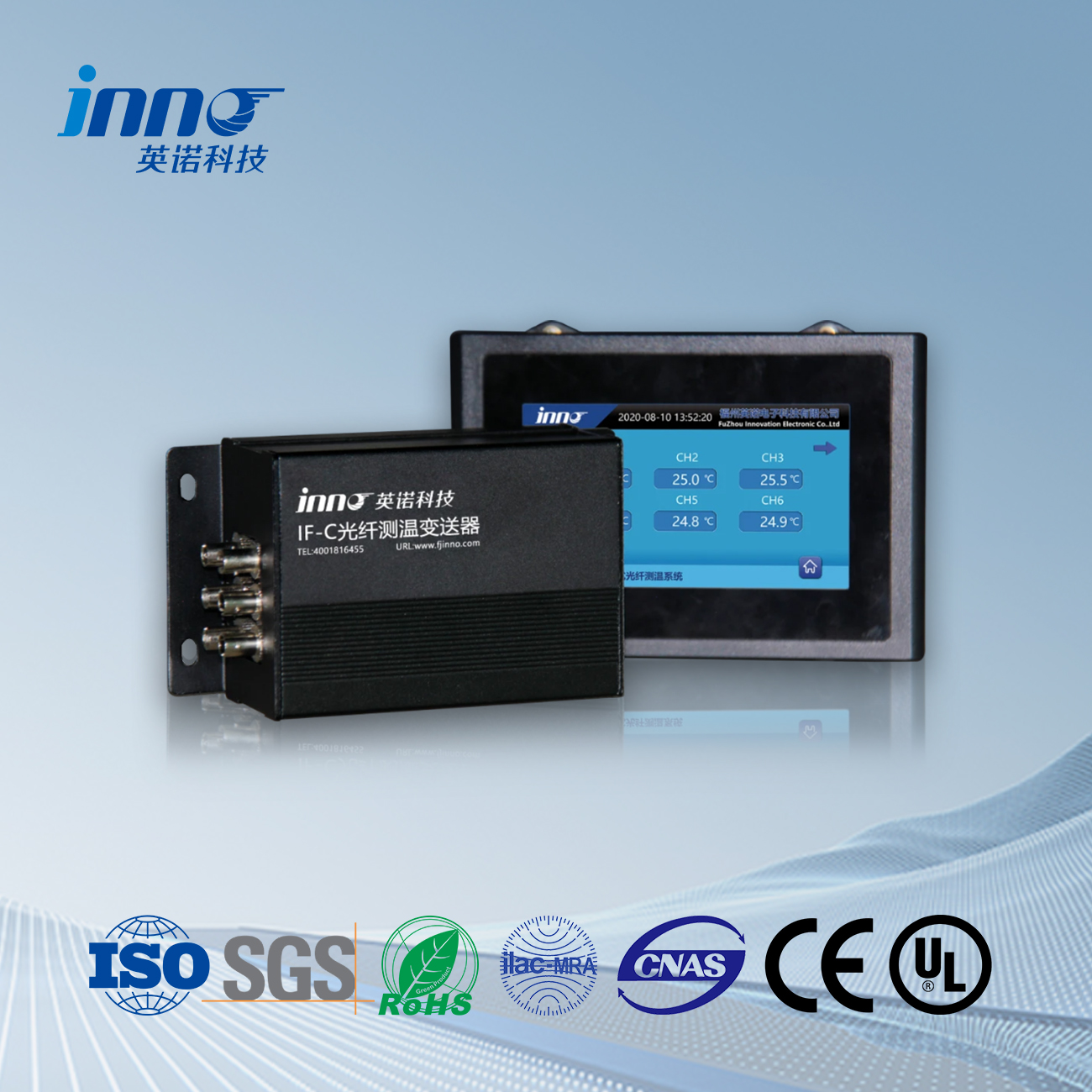
Glasvezeltemperatuursonde
De glasvezel temperatuursonde is the sensing element installed at the measurement point — on the ESC surface, inside the chamber wall, at the gas showerhead, or within a furnace tube. Probes are engineered in multiple configurations including straight, angled, surface-mount, and threaded housing styles to accommodate different tool mounting requirements.
Glasvezelkabel
A fluorescent optical fiber cable connects each probe to the demodulator. Cables are designed with protective jackets rated for the specific environment — high temperature, chemical exposure, or tight bend radius routing inside equipment frames.
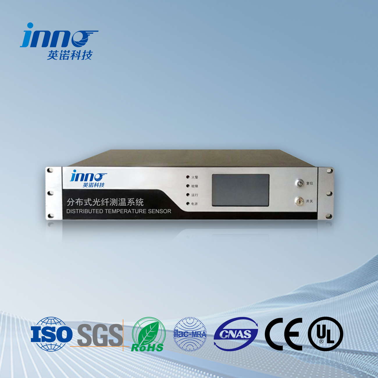
Fiber Optic Demodulator
De glasvezeldemodulator is the central signal processing instrument. It generates excitation light pulses, receives the fluorescent return signals, calculates temperature from decay time data, and outputs calibrated readings. Industrial-grade demodulators support multi-channel operation, allowing simultaneous monitoring of 4, 8, 16, or more sensor points from a single unit.
Communicatie en Integratie
Demodulators provide standard output interfaces including analog 4–20 mA, RS485, Modbus RTU/TCP, EtherNet/IP, and EtherCAT. This enables seamless integration with tool controllers, programmeerbare logische controllers (PLC's), and fab-wide manufacturing execution systems (MES) and fault detection and classification (FDC) platforms.
Software and Data Management
Monitoring software provides real-time display, trend charting, alarmbeheer, and historical data logging. Temperature data feeds into statistical process control (SPC) systems for ongoing process health assessment and supports root cause analysis when process excursions occur.
9. Toepassingen in halfgeleiderprocesstappen
Plasma-Enhanced CVD (PECVD)
PECVD deposits dielectric films such as SiO₂ and SiN at relatively low temperatures. The RF plasma environment makes fiber optic sensing essential. Glasvezel temperatuursensoren monitor pedestal temperature, chamber lid temperature, and gas line temperature to ensure film uniformity and stress control.
High-Density Plasma Etching
ICP and CCP etch tools remove material with nanometer-level precision. Wafer chuck temperature directly affects etch rate, profile angle, en selectiviteit. Fluorescerende glasvezelsensoren embedded in the ESC assembly provide real-time feedback for closed-loop temperature control unaffected by the intense plasma RF field.
Thermal Oxidation and Diffusion
Horizontal and vertical furnaces performing dry and wet oxidation, LPCVD, and dopant drive-in operate at high temperatures where precise multi-zone profiling is mandatory. Fiber optic sensors complement or replace legacy thermocouples in furnace profile monitoring to achieve tighter temperature uniformity across the wafer boat.
Rapid Thermal Processing (RTP)
RTP chambers ramp wafer temperature at rates exceeding 100 °C per second. Fast-response glasvezel temperatuursondes track these rapid transients accurately, supporting precise anneal and activation process control.
Sputtering and PVD
Magnetron sputtering systems generate strong magnetic and RF fields. Fiber optic sensors installed on the substrate chuck and near the target provide reliable temperature data where conventional sensors fail due to electromagnetic interference.
Advanced Packaging
Thermocompression bonding, solder reflow, molding compound cure, and underfill processes all depend on tightly controlled temperature profiles. Temperatuurbewaking via glasvezel ensures package-level reliability in fan-out wafer-level packaging (FOWLP), 2.5D, and 3D IC integration.
Wet Processing and CMP
Chemical bath temperature in wet etch and clean stations directly controls etch rate uniformity. CMP pad and slurry temperature influence removal rate and surface planarity. Fiber optic sensors withstand the chemical environment and deliver stable measurement in these applications.
10. Veelgestelde vragen over halfgeleidertemperatuurbewaking
Q1: Wat is halfgeleidertemperatuurbewaking?
Bewaking van de temperatuur van halfgeleiders is the continuous measurement and control of temperature at critical points throughout IC fabrication — including wafer surfaces, process chamber interiors, and equipment subsystems — to maintain process accuracy, protect equipment, and maximize wafer yield.
Vraag 2: Why are fiber optic sensors preferred in semiconductor fabs?
Fluorescerende glasvezeltemperatuursensoren are preferred because they are completely immune to RF and electromagnetic interference generated by plasma process tools, introduce zero metallic contamination risk in cleanroom environments, and resist the corrosive chemistries used in etch and deposition processes.
Q3: How does a fluorescent fiber optic temperature sensor work in a semiconductor tool?
The sensor probe’s phosphor tip is excited by a light pulse transmitted through the optical fiber. The resulting fluorescent afterglow decays at a rate that varies with temperature. De glasvezeldemodulator precisely measures this decay time and converts it to a calibrated temperature reading — all without any electrical signal at the measurement point.
Q4: Can fiber optic sensors operate inside plasma chambers?
Ja. Because the fiber and probe contain no metallic components, they do not interact with RF plasma fields. They operate reliably inside PECVD, etch, and PVD chambers where thermocouples and RTDs suffer from severe interference and contamination issues.
Vraag 5: What temperature range do semiconductor fiber optic sensors cover?
Standaard fluorescent fiber optic temperature probes cover ranges from −40 °C to +300 °C for most chamber and chuck applications. Specialized high-temperature probes extend to 400 °C or higher for furnace and RTP applications. Custom configurations are available for cryogenic applications.
Vraag 6: Do fiber optic sensors meet cleanroom contamination standards?
Ja. Probes and fiber cables are constructed from non-metallic, non-shedding materials such as glass, keramiek, PTFE, and PFA. They meet the particulate and ionic contamination requirements for use in ISO Class 1 to Class 5 cleanroom environments.
Vraag 7: How many channels can a single demodulator support?
Industrieel fiber optic demodulators zijn beschikbaar in ondersteunende configuraties 4, 8, 16, or more channels per unit. Meerdere eenheden kunnen met elkaar in een netwerk worden opgenomen om de monitoring over een gehele procestool of toolset te schalen.
Vraag 8: Hoe kunnen glasvezelmonitoringsystemen worden geïntegreerd met fabrieksautomatisering??
Demodulatoren communiceren via standaard industriële protocollen, waaronder RS485, Modbus RTU/TCP, EtherNet/IP, and EtherCAT. Temperatuurgegevens kunnen rechtstreeks worden geïntegreerd met gereedschapscontrollers, PLC's, MES, en FDC-platforms voor realtime procescontrole en statistische analyse.
Vraag 9: What maintenance do fiber optic temperature sensors require?
Fluorescerende glasvezelsensoren vereisen vrijwel geen onderhoud. Er is geen herkalibratieschema, geen verbruiksartikelen, en er zijn geen elektrische aansluitingen om te inspecteren. Sensoren werken doorgaans langer dan continu 10 jaar in productieomgevingen zonder degradatie.
Q10: Kunnen glasvezelsensoren bestaande thermokoppels in halfgeleidergereedschappen vervangen??
Ja. Glasvezeltemperatuursondes can be designed as drop-in replacements for existing thermocouple installations in many semiconductor tools. The probe form factor, mounting interface, and signal output can be matched to existing tool specifications, simplifying the retrofit process.
Vrijwaring: De informatie in dit artikel is uitsluitend bedoeld voor algemene informatieve en educatieve doeleinden. Hoewel er alles aan is gedaan om de nauwkeurigheid te garanderen, Fjinno makes no warranties or representations regarding the completeness or applicability of the content to any specific semiconductor process or equipment configuration. Productspecificaties, temperatuurbereiken, and system capabilities may vary depending on application requirements. For project-specific technical consultation and product selection, please contact the engineering team at www.fjinno.net. All product names, trademarks, and registered trademarks mentioned are the property of their respective owners.

Glasvezel temperatuursensor, Intelligent monitoringsysteem, Gedistribueerde glasvezelfabrikant in China
 |
 |
 |