 Sensor suhu serat optik INNO ,sistem pemantauan suhu.
- Pemantauan suhu semikonduktor adalah praktik mengukur dan mengendalikan suhu pada tingkat wafer, di dalam ruang proses, dan lintas subsistem peralatan untuk memastikan pengulangan proses, memaksimalkan hasil, dan melindungi komponen sensitif.
- Sensor suhu serat optik fluoresen secara unik cocok untuk lingkungan semikonduktor karena kebal terhadap interferensi elektromagnetik, bidang RF, dan energi plasma — semuanya umum pada alat proses yang luar biasa.
- Poin pemantauan penting meliputi ruang CVD, reaktor etsa, tungku difusi, Sistem sputtering PVD, tahapan litografi, Pembersih pelat CMP, dan wafer chuck.
- Sensor serat optik tidak menghasilkan kontaminasi logam, memenuhi standar partikulat ruang bersih yang ketat, dan tahan terhadap proses kimia korosif.
- Solusi pemantauan lengkap digabungkan probe suhu serat optik, A demodulator serat optik, pemrosesan sinyal multi-saluran, dan integrasi perangkat lunak dengan pengontrol alat dan platform MES/FDC yang luar biasa.
Daftar isi
- What Is Semiconductor Temperature Monitoring
- Why Temperature Control Matters in Semiconductor Manufacturing
- Key Temperature Monitoring Points in Fab Processes
- Challenges of Temperature Measurement in Semiconductor Tools
- Cara Kerja Sensor Serat Optik Fluoresen
- Advantages of Fiber Optic Sensors for Semiconductor Applications
- Fiber Optic vs Thermocouple vs RTD in Semiconductor Environments
- System Architecture of a Fiber Optic Monitoring Solution
- Applications Across Semiconductor Process Steps
- FAQs About Semiconductor Temperature Monitoring
1. Apa Semiconductor Temperature Monitoring

Definisi dan Ruang Lingkup
Pemantauan suhu semikonduktor refers to the measurement, rekaman, and control of temperature at every stage of integrated circuit fabrication where thermal conditions directly influence process outcomes. This encompasses wafer-level temperature during deposition, etsa, implantasi ion, oksidasi, and annealing, serta suhu dinding ruang proses, jalur pengiriman gas, potongan wafer, chuck elektrostatis (ESC), sirkuit air pendingin, dan sistem pembuangan. Data suhu yang akurat sangat penting untuk menjaga jendela proses ketat yang dibutuhkan node semikonduktor modern.
Peran Suhu dalam Fabrikasi IC
Hampir setiap langkah proses dalam pabrik semikonduktor sensitif terhadap panas. Keseragaman ketebalan film dalam pengendapan uap kimia bergantung pada suhu substrat. Tingkat etsa dan pergeseran selektivitas dengan suhu ruang dan wafer. Profil difusi dopan diatur oleh akurasi suhu tungku. Kontrol dimensi kritis dalam litografi dipengaruhi oleh stabilitas termal tahap reticle dan wafer. Dalam setiap kasus, penyimpangan suhu bahkan beberapa derajat dapat mendorong proses keluar dari spesifikasi, resulting in yield loss and scrap wafers.
From Periodic Checks to Continuous Monitoring
Secara historis, semiconductor temperature measurement relied on periodic thermocouple wafer runs or calibration checks. Modern fab operations have shifted toward continuous, real-time monitoring embedded directly into process tools. This transition enables tighter process control, faster fault detection, and higher overall equipment effectiveness.
2. Mengapa Temperature Control Matters in Semiconductor Manufacturing

Yield and Process Uniformity
Yield is the central metric of any semiconductor fab. Temperature non-uniformity across a wafer or between wafers in a batch directly translates to variation in film properties, line widths, junction depths, and device performance. Maintaining wafer temperature within a tolerance as tight as ±0.5 °C is essential at advanced nodes. Dapat diandalkan pemantauan suhu wafer system is the foundation for achieving this level of uniformity.
Perlindungan Peralatan
Process chambers, Generator RF, turbo pumps, and other subsystems are expensive and sensitive to thermal stress. Overheating of a showerhead, an ESC heater malfunction, or a cooling water flow interruption can cause immediate equipment damage. Waktu nyata chamber temperature monitoring provides the early warning needed to trigger interlocks and prevent costly tool downtime.
Advanced Node Requirements
As semiconductor manufacturing moves to smaller geometries, thermal budgets shrink and process sensitivity to temperature increases. Pada 7 nm, 5 nm, dan 3 nm nodes, even minor temperature excursions during gate oxide growth or high-k dielectric deposition can degrade device reliability. The demand for more precise, more responsive, and more interference-resistant temperature sensing continues to intensify.
Regulatory and Quality Compliance
Otomotif, Aerospace, and medical semiconductor products require full process traceability. Continuous temperature records from every process step form a critical part of the quality documentation and compliance audit trail required by standards such as IATF 16949 dan ISO 13485.
3. Key Temperature Monitoring Points in Fab Processes
Chemical Vapor Deposition (CVD) Chambers
In both LPCVD and PECVD systems, CVD temperature monitoring covers the wafer susceptor or pedestal, dinding ruang, gas inlet showerhead, and exhaust line. Susceptor temperature directly controls deposition rate and film quality. Wall temperature affects particle generation and precursor condensation. Sensor suhu serat optik fluoresen placed at these locations deliver accurate readings unaffected by the RF plasma field inside the chamber.
Etching Reactors
Plasma etch tools — including reactive ion etching (RIE), inductively coupled plasma (ICP), and capacitively coupled plasma (CCP) systems — expose sensors to intense RF energy, corrosive fluorine and chlorine chemistries, and rapid thermal cycling. Etching chamber temperature sensors based on fiber optic technology survive this environment while providing stable readings that metallic sensors cannot match.
Diffusion and Oxidation Furnaces
Horizontal and vertical tungku difusi operate at temperatures from 800 °C to over 1200 °C. Multi-zone temperature profiling ensures uniform thermal treatment across all wafers in the boat. Diffusion furnace temperature monitoring with high-accuracy sensors is essential for consistent oxide growth, drive-in diffusion, and anneal processes.
Physical Vapor Deposition (PVD) Sistem
Sputtering and evaporation tools require monitoring of target temperature, substrate chuck temperature, and chamber wall temperature. Magnetron sputtering generates strong magnetic fields that interfere with conventional metallic sensors, membuat sensor suhu serat optik the preferred choice.
Lithography and Metrology Stages
Thermal stability of the wafer stage, reticle stage, and projection lens assembly is critical for overlay accuracy and CD control. Even sub-degree temperature changes can cause thermal expansion that shifts alignment. Fiber optic sensors embedded in stage structures provide the non-contact, EMI-free measurement these precision systems require.
CMP, Wet Bench, and Packaging
Chemical mechanical planarization pad and slurry temperature affects removal rate. Wet bench chemical bath temperature controls etch uniformity. In advanced packaging processes such as thermocompression bonding and reflow soldering, precise temperature profiling ensures reliable interconnects. Fiber optic monitoring supports all of these applications.
4. Challenges of Temperature Measurement in Semiconductor Tools
Strong Electromagnetic and RF Interference
Plasma-based process tools generate powerful RF fields at frequencies from hundreds of kilohertz to tens of megahertz. These fields induce noise and errors in conventional metallic temperature sensors. Any sensor with electrical conductors — thermocouples, RTD, or thermistors — is susceptible to significant measurement drift when exposed to RF energy. This is the single greatest challenge for accurate semiconductor process temperature control and the primary reason fiber optic sensing has gained adoption.
Contamination Sensitivity
Semiconductor cleanrooms operate at ISO Class 1 to Class 5 tingkat. The introduction of metallic particles from sensor leads, solder joints, or corroded sheaths can contaminate wafers and destroy device yield. Sensors used inside or near process chambers must be constructed from non-metallic, non-shedding materials that meet fab cleanliness standards.
Corrosive and Aggressive Chemistries
Process gases including NF₃, CF₄, Cl₂, HBr, and NH₃ are highly corrosive. Wet process chemicals such as HF, H₂SO₄, and SC-1/SC-2 solutions attack many conventional sensor materials. Temperature sensors in these environments must resist chemical degradation over extended service periods.
Extreme Temperature Ranges
Semiconductor processes span a wide range — from cryogenic wafer chucks operating below −40 °C in certain etch processes to diffusion furnaces exceeding 1200 °C. A single sensing technology that covers a broad range simplifies standardization across the fab.
Batasan Ruang
Alat proses modern penuh dengan komponen. Sensor harus secara fisik cukup kecil agar dapat ditempatkan di ruang terbatas seperti rakitan ESC, rumah pancuran, dan perlengkapan saluran gas tanpa mengganggu dinamika aliran gas atau fungsi mekanis.
5. Cara Kerja Sensor Serat Optik Fluoresen

Pengukuran Waktu Peluruhan Fluoresensi
Sebuah sensor suhu serat optik neon beroperasi berdasarkan prinsip fotoluminesensi. Ujung probe serat optik dilapisi dengan bahan fosfor tanah jarang. Pulsa cahaya eksitasi bergerak melalui serat dan menstimulasi fosfor. Fosfor memancarkan pijaran fluoresen yang waktu peluruhannya tepat, fungsi suhu yang dapat diulang. Si demodulator serat optik mengukur waktu peluruhan ini dengan resolusi tinggi dan mengubahnya menjadi keluaran suhu yang dikalibrasi.
Mengapa Waktu Peluruhan dan Bukan Intensitas
Mengukur waktu peluruhan dibandingkan intensitas fluoresensi membuat sensor secara inheren kebal terhadap variasi amplitudo sinyal yang disebabkan oleh hilangnya pembengkokan serat, penuaan konektor, atau fluktuasi sumber cahaya. Hal ini memberikan sensor serat optik fluoresen dengan stabilitas jangka panjang yang luar biasa tanpa perlu sering melakukan kalibrasi ulang — sebuah keuntungan yang menentukan dalam lingkungan produksi yang luar biasa..
Jalur Sinyal Optik Murni
Dari ujung probe hingga demodulator, seluruh rantai penginderaan bersifat optik. Tidak ada sinyal listrik, tidak ada konduktor logam, dan tidak ada komponen elektronik aktif pada atau di dekat titik pengukuran. Ini menghilangkan pengambilan RF, loop tanah, dan memicu risiko, dan menyediakan isolasi galvanik lengkap antara sensor dan instrumentasi.
6. Advantages of Fiber Optic Sensors for Semiconductor Applications
Kekebalan RF dan EMI Lengkap
Karena serat optik dan probe sepenuhnya non-konduktif, sensor suhu serat optik adalah 100% kebal terhadap medan RF, interferensi elektromagnetik, dan transien tegangan tinggi. Akurasi pengukuran tetap tidak berubah terlepas dari daya plasma atau frekuensi RF yang digunakan. Hal ini menjadikan mereka solusi pasti pemantauan suhu semikonduktor di dalam ruang plasma.
Risiko Kontaminasi Logam Nol
Probe dan serat dibuat dari kaca, keramik, dan bahan fluoropolimer. Tidak ada logam yang hadir pada titik penginderaan. Hal ini menghilangkan risiko timbulnya partikel logam atau kontaminasi ionik — yang merupakan persyaratan mendasar dalam aplikasi pelapis wafer.
Ketahanan Kimia dan Plasma
Enkapsulasi probe menggunakan PTFE, PFA, kuarsa, dan keramik tahan terhadap bahan kimia agresif dan pemboman plasma yang ditemui dalam proses etsa, CVD, dan proses bersih. Sensor menjaga akurasi dan integritas fisik selama ribuan siklus proses.
Desain Probe yang Ringkas
Pemeriksaan suhu serat optik tersedia dengan diameter luar sekecil 1 Mm, allowing installation in the tightest spaces inside semiconductor equipment without affecting gas flow patterns or mechanical clearances.
Waktu Respon Cepat
Small thermal mass at the probe tip delivers response times on the order of milliseconds to hundreds of milliseconds, enabling real-time tracking of rapid thermal transients during plasma strikes, lamp ramp-ups, and process step transitions.
Umur Panjang dan Perawatan Rendah
With no moving parts, no electrical connections at the probe, and no drift mechanisms, fluorescent fiber optic sensors routinely deliver service lives exceeding 10 years in continuous production use. Maintenance requirements are minimal, reducing the total cost of ownership compared with conventional sensor technologies.
7. Fiber Optic vs Thermocouple vs RTD in Semiconductor Environments
Thermocouple Limitations
Thermocouples are low cost and widely available, but their metallic construction makes them fundamentally incompatible with high-RF semiconductor environments. RF pickup introduces measurement errors that can exceed several degrees. Metallic junctions are contamination sources. Thermocouple accuracy degrades over time due to oxidation and diffusion of junction materials at elevated temperatures.
RTD Limitations
Platinum RTDs offer better baseline accuracy than thermocouples but share the same vulnerability to RF interference through their metallic lead wires. Shielding and filtering add bulk and complexity, and these mitigation measures are often insufficient inside high-power plasma chambers. RTDs also carry contamination risk in cleanroom environments.
Fiber Optic Sensor Advantages in Direct Comparison
Sensor suhu serat optik fluoresen eliminate every disadvantage of metallic sensors in semiconductor applications. They are RF-immune, contamination-free, chemically resistant, padat, dan bebas perawatan. While the per-unit sensor cost is higher than a basic thermocouple, the total cost of ownership is lower when factoring in measurement reliability, reduced yield loss, lower maintenance burden, dan masa pakai lebih lama.
Tabel Perbandingan
| Parameter | Sensor Serat Optik | Termokopel | RTD (PT100) |
|---|---|---|---|
| RF/EMI Immunity | Menyelesaikan | Miskin | Miskin |
| Metallic Contamination | Tidak ada | Risiko tinggi | Moderate risk |
| Ketahanan Kimia | Bagus sekali | Terbatas | Terbatas |
| Ketepatan | ±0,3–0,5 °C | ±1–2 °C | ±0,5 °C |
| Stabilitas Jangka Panjang | Bagus sekali | Miskin | Sedang |
| Ukuran Pemeriksaan | Very compact | Kompak | Larger with shielding |
| Cleanroom Compatibility | Penuh | Terbatas | Terbatas |
| Kehidupan Pelayanan | 10+ Tahun | 1–3 years | 3–5 years |
8. System Architecture of a Fiber Optic Monitoring Solution
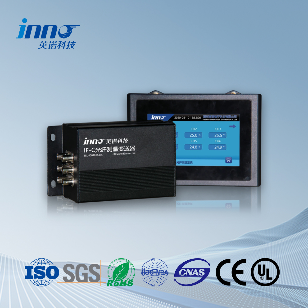
Pemeriksaan Suhu Serat Optik
Si pemeriksaan suhu serat optik is the sensing element installed at the measurement point — on the ESC surface, inside the chamber wall, at the gas showerhead, or within a furnace tube. Probes are engineered in multiple configurations including straight, angled, pemasangan di permukaan, and threaded housing styles to accommodate different tool mounting requirements.
Kabel Serat Optik
Sebuah fluorescent optical fiber cable connects each probe to the demodulator. Cables are designed with protective jackets rated for the specific environment — high temperature, paparan bahan kimia, or tight bend radius routing inside equipment frames.
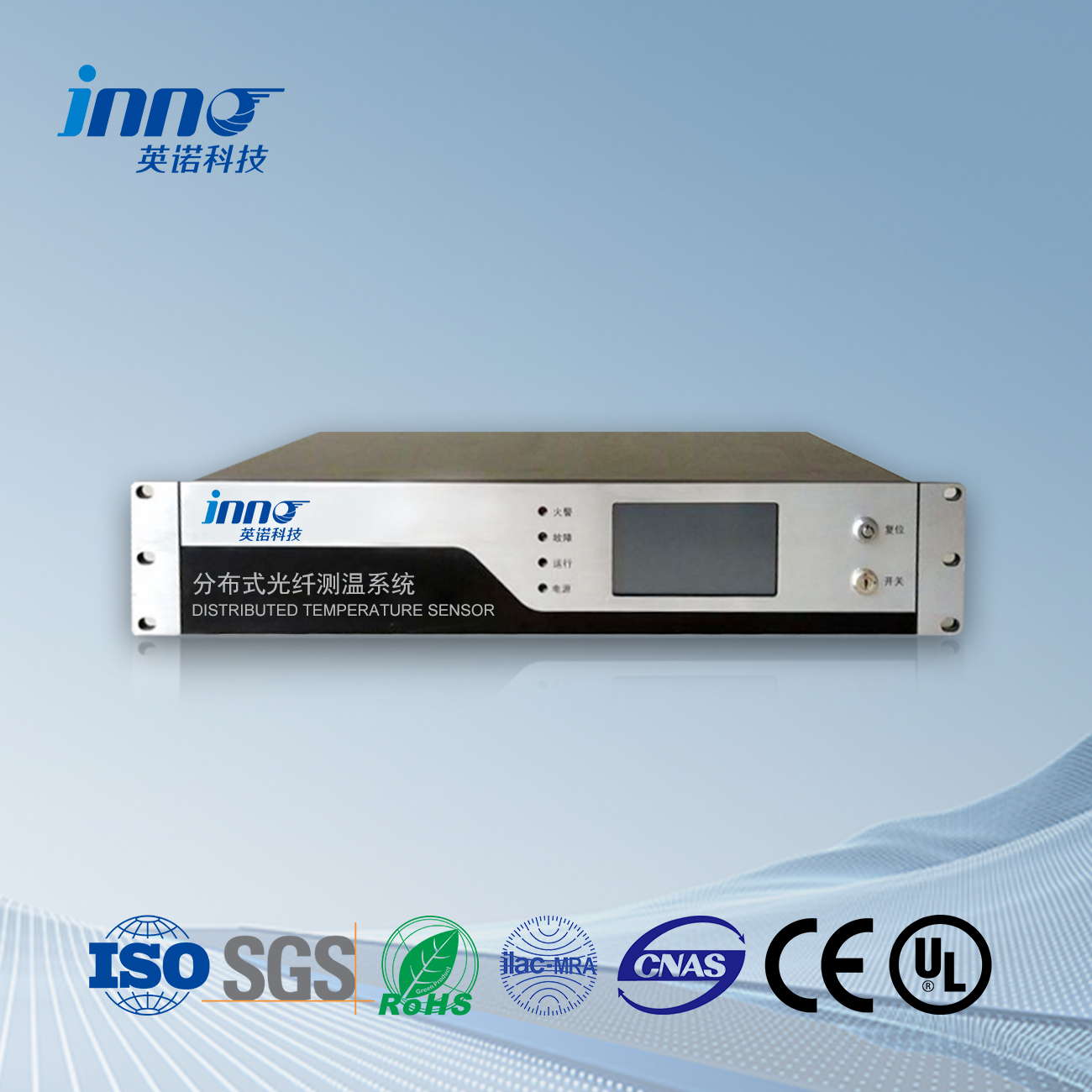
Demodulator Serat Optik
Si demodulator serat optik is the central signal processing instrument. It generates excitation light pulses, receives the fluorescent return signals, calculates temperature from decay time data, and outputs calibrated readings. Industrial-grade demodulators support multi-channel operation, allowing simultaneous monitoring of 4, 8, 16, or more sensor points from a single unit.
Komunikasi dan Integrasi
Demodulators provide standard output interfaces including analog 4–20 mA, RS485, Modbus RTU/TCP, EtherNet/IP, and EtherCAT. This enables seamless integration with tool controllers, pengontrol logika yang dapat diprogram (PLC), and fab-wide manufacturing execution systems (MES) and fault detection and classification (FDC) platform.
Software and Data Management
Monitoring software provides real-time display, trend charting, manajemen alarm, and historical data logging. Temperature data feeds into statistical process control (SPC) systems for ongoing process health assessment and supports root cause analysis when process excursions occur.
9. Applications Across Semiconductor Process Steps
Plasma-Enhanced CVD (PECVD)
PECVD deposits dielectric films such as SiO₂ and SiN at relatively low temperatures. The RF plasma environment makes fiber optic sensing essential. Sensor suhu serat optik monitor pedestal temperature, chamber lid temperature, and gas line temperature to ensure film uniformity and stress control.
High-Density Plasma Etching
ICP and CCP etch tools remove material with nanometer-level precision. Wafer chuck temperature directly affects etch rate, profile angle, dan selektivitas. Sensor serat optik neon embedded in the ESC assembly provide real-time feedback for closed-loop temperature control unaffected by the intense plasma RF field.
Thermal Oxidation and Diffusion
Horizontal and vertical furnaces performing dry and wet oxidation, LPCVD, and dopant drive-in operate at high temperatures where precise multi-zone profiling is mandatory. Fiber optic sensors complement or replace legacy thermocouples in furnace profile monitoring to achieve tighter temperature uniformity across the wafer boat.
Pemrosesan Termal yang Cepat (RTP)
RTP chambers ramp wafer temperature at rates exceeding 100 °C per second. Fast-response probe suhu serat optik track these rapid transients accurately, supporting precise anneal and activation process control.
Sputtering and PVD
Magnetron sputtering systems generate strong magnetic and RF fields. Fiber optic sensors installed on the substrate chuck and near the target provide reliable temperature data where conventional sensors fail due to electromagnetic interference.
Advanced Packaging
Thermocompression bonding, solder reflow, molding compound cure, and underfill processes all depend on tightly controlled temperature profiles. Pemantauan suhu serat optik ensures package-level reliability in fan-out wafer-level packaging (FOWLP), 2.5D, and 3D IC integration.
Wet Processing and CMP
Chemical bath temperature in wet etch and clean stations directly controls etch rate uniformity. CMP pad and slurry temperature influence removal rate and surface planarity. Fiber optic sensors withstand the chemical environment and deliver stable measurement in these applications.
10. FAQs About Semiconductor Temperature Monitoring
Q1: Apa itu pemantauan suhu semikonduktor?
Pemantauan suhu semikonduktor is the continuous measurement and control of temperature at critical points throughout IC fabrication — including wafer surfaces, process chamber interiors, and equipment subsystems — to maintain process accuracy, protect equipment, and maximize wafer yield.
Q2: Why are fiber optic sensors preferred in semiconductor fabs?
Sensor suhu serat optik fluoresen are preferred because they are completely immune to RF and electromagnetic interference generated by plasma process tools, introduce zero metallic contamination risk in cleanroom environments, and resist the corrosive chemistries used in etch and deposition processes.
Q3: How does a fluorescent fiber optic temperature sensor work in a semiconductor tool?
The sensor probe’s phosphor tip is excited by a light pulse transmitted through the optical fiber. The resulting fluorescent afterglow decays at a rate that varies with temperature. Si demodulator serat optik precisely measures this decay time and converts it to a calibrated temperature reading — all without any electrical signal at the measurement point.
Q4: Can fiber optic sensors operate inside plasma chambers?
Ya. Because the fiber and probe contain no metallic components, mereka tidak berinteraksi dengan bidang plasma RF. Mereka beroperasi dengan andal di dalam PECVD, mengetsa, dan ruang PVD tempat termokopel dan RTD mengalami gangguan parah dan masalah kontaminasi.
Q5: Berapa kisaran suhu yang dicakup oleh sensor serat optik semikonduktor?
Standar probe suhu serat optik fluoresen tutupan berkisar antara −40 °C hingga +300 °C untuk sebagian besar aplikasi ruang dan chuck. Probe suhu tinggi khusus meluas hingga 400 °C atau lebih tinggi untuk aplikasi tungku dan RTP. Konfigurasi khusus tersedia untuk aplikasi kriogenik.
Q6: Apakah sensor serat optik memenuhi standar kontaminasi ruang bersih?
Ya. Probe dan kabel serat dibuat dari non-logam, bahan yang tidak mudah rontok seperti kaca, keramik, PTFE, dan PFA. Mereka memenuhi persyaratan kontaminasi partikulat dan ionik untuk digunakan dalam Kelas ISO 1 to Class 5 lingkungan ruang bersih.
Q7: How many channels can a single demodulator support?
Industri demodulator serat optik are available in configurations supporting 4, 8, 16, or more channels per unit. Multiple units can be networked together to scale monitoring across an entire process tool or tool set.
Q8: How do fiber optic monitoring systems integrate with fab automation?
Demodulators communicate via standard industrial protocols including RS485, Modbus RTU/TCP, EtherNet/IP, and EtherCAT. Temperature data integrates directly with tool controllers, PLC, MES, and FDC platforms for real-time process control and statistical analysis.
Q9: Perawatan apa yang dibutuhkan sensor suhu serat optik?
Fluorescent fiber optic sensors require virtually no maintenance. There is no recalibration schedule, no consumable parts, and no electrical connections to inspect. Sensors typically operate continuously for over 10 years in production environments without degradation.
Q10: Can fiber optic sensors replace existing thermocouples in semiconductor tools?
Ya. Pemeriksaan suhu serat optik can be designed as drop-in replacements for existing thermocouple installations in many semiconductor tools. The probe form factor, mounting interface, and signal output can be matched to existing tool specifications, simplifying the retrofit process.
Penafian: Informasi yang diberikan dalam artikel ini hanya untuk tujuan informasi umum dan pendidikan. Meskipun segala upaya telah dilakukan untuk memastikan keakuratan, Fjinno makes no warranties or representations regarding the completeness or applicability of the content to any specific semiconductor process or equipment configuration. Spesifikasi produk, Kisaran suhu, and system capabilities may vary depending on application requirements. For project-specific technical consultation and product selection, silakan hubungi tim teknik di www.fjinno.net. Semua nama produk, merek dagang, and registered trademarks mentioned are the property of their respective owners.

Sensor suhu serat optik, Sistem pemantauan cerdas, Produsen serat optik terdistribusi di Cina
 |
 |
 |