 INNO 光ファイバー温度センサー ,温度監視システム.
重要なポイント
- 重要な温度管理: GOF 半導体製造では、製品の品質と歩留まりの最適化のために正確な熱管理が必要です
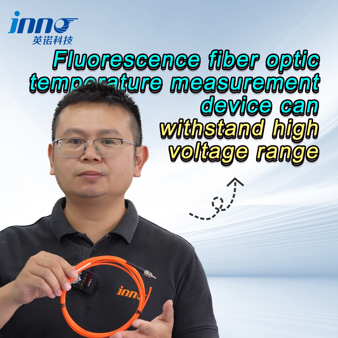
- 電磁波耐性: 蛍光光ファイバーセンサーはRFプラズマの影響を受けません, 高電圧, 工場環境における電磁干渉
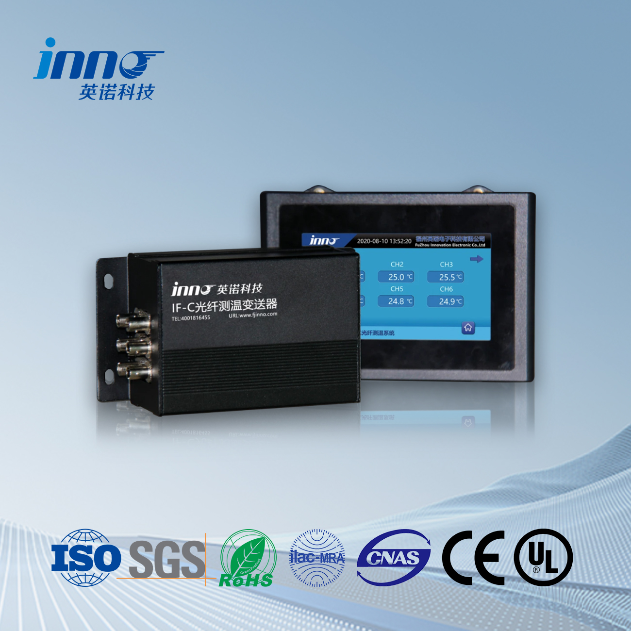
- 多地点監視: 単一の送信機をサポート 1-64 チャンネル 0-80 広範囲をカバーする伝送距離メーター
- 高電圧耐性: 完全な電気絶縁により、極度の電圧環境でも安全に動作可能
- 迅速な対応: 1 秒未満の応答時間 (<1s) リアルタイムのプロセス制御と機器保護を保証します
GOF 半導体温度監視の課題

GOF 半導体製造について理解する
絶縁体上の酸化ガリウム (ゴフ) semiconductor technology represents the cutting edge of power electronics and high-frequency devices. These advanced materials require ultra-precise fabrication processes where temperature control directly impacts device performance, 信頼性, and production yield. 主役として メーカー の 光ファイバー温度センサー, we understand the unique thermal management challenges in GOF semiconductor fabrication.
Critical Nature of Temperature Control
Temperature deviations of just a few degrees during deposition, エッチング, or annealing processes can compromise material properties, causing defects that render devices non-functional. Process temperatures typically range from room temperature to over 1000°C across different fabrication steps. 精度を±0.5℃以内に維持することは、一貫した製品品質と高価なウェーハの歩留まりを最大化するために不可欠であることがわかります。.
過酷な測定環境
半導体製造装置は温度測定にとって非常に困難な条件を作り出します. 高出力 RF 発生器は、プラズマ処理中に強力な電磁場を生成します。. 真空チャンバーは 10⁻⁹ torr までの圧力で動作します. 化学蒸気や反応性ガスがセンサー材料を攻撃する. 数千ボルトを超える高電圧システムは安全上の問題を引き起こす. 伝統的 温度測定装置 このような環境では苦戦するか完全に失敗する.
従来の温度センサーが半導体工場で失敗する理由

熱電対の干渉問題
While thermocouples offer broad temperature ranges, their metallic construction makes them susceptible to electromagnetic interference from RF plasma systems. Induced currents corrupt readings and can cause measurement errors exceeding 10-20°C during plasma processing. Metal components also introduce contamination risks in ultra-clean fabrication environments.
Thermistor Voltage Limitations
Thermistors require electrical current for operation, creating multiple problems in semiconductor applications. High voltage environments pose electrical safety hazards while RF fields induce noise that degrades accuracy. Lead wires act as antennas, picking up interference that makes reliable measurements impossible during critical process steps.
Infrared Thermometry Blind Spots
Non-contact infrared measurement avoids some interference issues but suffers from fundamental limitations. IR sensors cannot measure through vacuum chamber viewports accurately due to transmission losses and reflection errors. Surface-only measurement provides no information about internal substrate or wafer temperatures critical for process control. Emissivity variations across different materials further compromise accuracy.
光ファイバー温度センサー: The Optimal Solution for Semiconductor Manufacturing
完全な電磁耐性
専門家として 光ファイバー温度センサー メーカー, 私たちの 蛍光光ファイバーセンサー transmit temperature data as optical signals completely immune to electromagnetic interference. Whether RF plasma operates at kilowatts or electromagnetic fields fluctuate wildly, measurement accuracy remains unaffected. This immunity makes optical fiber temperature monitoring the only reliable solution for plasma processing equipment.
測定精度と安定性
私たちの 光ファイバー温度測定システム achieve ±0.5°C accuracy across their full measurement range. The fluorescence lifetime measurement principle ensures long-term stability without calibration drift. Unlike intensity-based sensors affected by fiber bending or connector degradation, lifetime measurements depend solely on fluorescent crystal temperature, maintaining accuracy throughout years of continuous operation.
Multi-Point Temperature Monitoring
A single compact 送信機 サポートします 1-64 測定チャンネル, enabling comprehensive spatial temperature mapping throughout processing equipment. と 0-80 meter transmission distance, センサーは重要な測定ポイントに設置され、信号処理電子機器は汚染区域または危険区域の外に安全に保管されます。. これ マルチチャンネル光ファイバーソリューション ポイントセンサーでは不可能な完全な熱プロファイリングを提供します.
高電圧耐性
完全な電気的絶縁は、半導体アプリケーションにとって重要な利点となります. 私たちの 光ファイバー温度プローブ 導電性材料を一切含まない - 純粋なシリカガラス繊維と非金属の感知素子により電気経路が排除されます。. この設計により、10kV を超える高電圧環境でもアーク放電の危険なく安全に動作できます。, 短絡, または従来のセンサーを悩ませるオペレーターの危険.
超高速の応答時間
プロセス制御にはリアルタイムの温度フィードバックが必要です. 私たちの 光ファイバーセンサー 1 秒未満の応答時間を実現 (<1s), 熱逸脱の即時検出と迅速な制御システム調整を可能にします。. This fast response protects expensive wafers from thermal damage and ensures process parameters remain within specification throughout each fabrication step.
Compact and Cleanroom Compatible
Miniaturized probe designs with diameters below 0.5mm integrate easily into crowded equipment interiors without disrupting gas flows or plasma uniformity. Non-outgassing materials maintain ultra-high vacuum compatibility while particle-free construction meets Class 1 cleanroom requirements. As both サプライヤー そして 工場, we engineer every component for semiconductor fab compatibility.
GOF 半導体製造における主な用途
Plasma Etching Temperature Monitoring
Plasma etching removes material through energetic ion bombardment, generating substantial heat. Wafer temperature directly affects etch rate, profile, と選択性. 私たちの 光ファイバー温度センサー mount directly to wafer chucks or chamber walls, providing accurate feedback for RF power and cooling system control. This real-time monitoring prevents thermal damage while optimizing etch uniformity across the wafer.
Chemical Vapor Deposition Temperature Control
CVD processes deposit thin films by decomposing precursor gases at precise temperatures. Film properties including composition, ストレス, and crystallinity depend critically on deposition temperature. 私たちの 多点監視システム measure temperature across heated susceptors, ensuring uniform conditions that produce consistent, high-quality films essential for device performance.
Wafer Annealing Process Monitoring
Thermal annealing activates dopants, ストレスを和らげる, 慎重に制御された加熱と冷却のサイクルにより結晶化度が向上します。. 大型ウェーハ全体の温度均一性が重要であることが判明しています。 光ファイバー温度測定装置 均一な加熱を検証し、これらの重要な熱サイクル中にウェーハの反りや亀裂を引き起こす可能性のあるホットスポットを検出する複数の測定ポイントを提供します.
真空チャンバーの温度管理
処理チャンバーの壁には、望ましくない堆積を防止し、プロセスの安定性を維持するために温度制御が必要です. 私たちの 卸売光ファイバーセンサー チャンバー内部全体に設置, 適切な調整を確保するために壁の温度を監視する. これにより、再現性のある処理結果に必要な熱環境を維持しながら、剥離堆積物による粒子の発生を防ぎます。.
RF 電力システムのモニタリング
High-power RF generators and matching networks generate significant heat that affects impedance matching and power delivery efficiency. 私たちの カスタマイズされた温度監視ソリューション track component temperatures in these high-voltage systems, enabling cooling system optimization and preventing equipment failures that cause costly production downtime.
半導体プロセスの技術的利点
真空対応性
私たちの 光ファイバー温度プローブ operate reliably from atmospheric pressure to ultra-high vacuum (UHV) conditions below 10⁻⁹ torr. Non-outgassing materials prevent chamber contamination while maintaining measurement accuracy across the full pressure range. This vacuum compatibility makes them ideal for deposition, エッチング, およびイオン注入装置.
Ultra-Clean Environment Suitability
Semiconductor fabs maintain stringent cleanliness standards where even minute contamination causes yield losses. Our sensors meet ISO Class 1 cleanroom requirements with particle-free designs and materials compatible with aggressive cleaning chemistries. As a trusted サプライヤー, we validate every product for fab compatibility before delivery.
長期安定性
The fluorescence lifetime measurement principle provides inherent stability without calibration drift. 私たちの 光ファイバーセンシングシステム maintain factory accuracy for years of continuous operation, eliminating downtime for calibration procedures. This stability reduces maintenance costs while ensuring consistent process control throughout equipment lifetimes.
Extended Transmission Distance
と 0-80 meter transmission capability, 私たちの 光ファイバー温度トランスミッター can be located in clean, controlled environments while sensors operate inside contaminated process chambers. This separation protects electronics from corrosive gases and high temperatures while simplifying maintenance and reducing equipment footprint in expensive fab space.
耐薬品性
シリカガラス繊維は、フッ素ベースのエッチャントを含むほとんどの半導体プロセス化学薬品による攻撃に耐性があります。, 酸化剤, および腐食性蒸気. この耐薬品性により、従来のセンサーが急速に劣化する過酷な環境でも信頼性の高い動作が保証されます。, 長寿命を実現し、交換コストを削減します.
半導体アプリケーション向けの温度センサー技術の比較
| 特徴 | 蛍光光ファイバー | 熱電対 | サーミスター | 赤外線 |
|---|---|---|---|---|
| EMI耐性 | 完了 | 貧しい | 貧しい | 良い |
| 正確さ | ±0.5℃ | ±1~2℃ | ±0.5℃ | ±2~5℃ |
| 応答時間 | <1 2番 | 1-2 秒 | 2-5 秒 | インスタント |
| 高電圧の安全性 | 素晴らしい | 貧しい | 貧しい | 良い |
| 真空対応 | はい (UHVへ) | 限定 | 限定 | 連絡がありません |
| マルチポイント機能 | 1-64 チャンネル | シングルポイント | シングルポイント | シングルポイント |
| 校正が必要です | いいえ | 定期的 | 定期的 | 定期的 |
| クリーンルーム対応 | クラス 1 | 限定 | 限定 | はい |
| 内部測定 | はい | はい | はい | 表面のみ |
世界の半導体産業のアプリケーション
中東の半導体施設
私たちの 光ファイバー温度監視システム 中東地域の複数の半導体工場にサービスを提供. アラブ首長国連邦の主要施設は、包括的な CVD チャンバー監視に当社の 32 チャンネル システムを使用しています, 達成する 15% 温度均一性の向上による収量の向上. サウジアラビアの研究機関が先端材料開発に当社のセンサーを採用, leveraging electromagnetic immunity for novel plasma processing techniques.
Southeast Asian Manufacturing Hubs
主役として 輸出者, we supply numerous Southeast Asian semiconductor manufacturers. Singapore’s advanced packaging facilities integrate our 光学式温度センサー into flip-chip bonding equipment for precise thermal control. Malaysian LED manufacturers use our systems to monitor MOCVD reactor temperatures, improving device brightness uniformity. Thailand’s automotive chip producers rely on our sensors for power semiconductor fabrication requiring exact thermal management.
European Advanced Manufacturing
European semiconductor research centers utilize our customized fiber optic solutions for next-generation device development. German institutes developing wide-bandgap semiconductors employ our high-temperature sensors for SiC and GaN processing. French photonics manufacturers integrate our multi-point monitoring into laser diode fabrication lines.
North American Production Lines
US semiconductor fabs deploy our bulk fiber optic temperature systems across production lines. Major foundries use our sensors for 300mm wafer processing equipment, benefiting from calibration-free operation that reduces maintenance costs. Canadian MEMS manufacturers rely on our vacuum-compatible sensors for microstructure fabrication requiring sub-degree temperature control.
メーカー & Custom Temperature Monitoring Solutions
Professional Manufacturing Capabilities
FJINNO operates as a specialized 光ファイバー温度センサーのメーカー そして 工場 serving the global semiconductor industry. Our production facility implements rigorous quality standards ensuring every 送信機 and sensor meets demanding fab requirements. We function as both direct サプライヤー そして 輸出者, delivering worldwide.
Tailored OEM/ODM Services
We provide comprehensive OEM/ODM ソリューション for equipment manufacturers integrating temperature monitoring into semiconductor tools. Our capabilities include custom channel configurations, specialized probe designs for unique applications, そして プライベートブランド ブランディング. Engineering support ensures seamless integration with your equipment.
Volume Supply Programs
As a direct 工場, we offer competitive pricing for 卸売 そして バルク orders. 販売代理店 そして ディーラー benefit from volume discounts, 技術研修, and marketing support. 私たちの カスタマイズされた solutions address specific application requirements while maintaining cost-effectiveness.
Frequently Asked Questions About Fluorescent Fiber Optic Temperature Sensors
How do fluorescent fiber optic temperature sensors work?
蛍光光ファイバーセンサー use rare earth crystals that emit fluorescence when illuminated. 蛍光の減衰時間は温度によって変化します。この寿命測定により、光の強度に完全に依存せずに正確な温度測定値が得られます。, ファイバー損失, またはコネクタの品質. この原理により、校正を必要とせずに長期的な安定性が保証されます。.
光ファイバーセンサーは真空環境でも動作できますか?
はい, 私たちの 光ファイバー温度プローブ operate reliably from atmospheric pressure to ultra-high vacuum (UHV) 10⁻⁹トル以下. 非放出ガス材料によりチャンバーの汚染を防ぎ、すべての圧力範囲にわたって完全な精度を維持します, 半導体蒸着装置やエッチング装置に最適です。.
センサーはどの温度範囲をカバーしますか?
標準的な半導体グレードのセンサーは -40°C ~ +300°C を測定します, ほとんどの製造プロセスをカバー. 私たちは提供します カスタム 特殊な用途向けの製品範囲. として メーカー, 特定の温度ウィンドウに最適化されたセンサーを設計します, プロセスの精度を最大化する.
Do fluorescent fiber optic sensors require calibration?
いいえ, this represents a key advantage of 蛍光光ファイバー温度センサー. The fluorescence lifetime measurement principle provides inherent stability without drift. Sensors maintain factory accuracy for years of continuous operation, eliminating calibration downtime and associated costs—critical for high-volume semiconductor manufacturing.
How many measurement points can one system monitor?
私たちの 光ファイバー温度トランスミッター サポート 1-64 ユニットあたりのチャンネル数. Each fiber monitors one point, but multi-channel systems enable comprehensive spatial temperature mapping throughout processing equipment. Networked configurations provide hundreds of measurement points for fab-wide monitoring.
Can the system integrate with existing semiconductor equipment?
絶対に. 私たちの OEM solutions feature standard industrial protocols (RS-485, イーサネット, Modbus, アナログ出力) for seamless integration with equipment controllers and fab automation systems. We provide complete integration support and documentation as part of our サプライヤー サービス.
What makes fiber optic sensors better than thermocouples for semiconductor applications?
光ファイバー温度監視 offers complete electromagnetic immunity, essential for RF plasma environments where thermocouples fail. Our sensors tolerate high voltages safely, require no calibration, support multi-point monitoring from a single transmitter, and maintain cleanroom compatibility—advantages impossible with conventional sensors.
Contact FJINNO for Semiconductor Temperature Monitoring Solutions
福州イノベーション電子科学&テック株式会社, 株式会社. specializes in manufacturing 蛍光光ファイバー温度センサー for semiconductor and advanced manufacturing applications. 主役として メーカー, サプライヤー, そして 輸出者, we provide complete temperature monitoring solutions serving fabs worldwide.
当社の製品範囲には以下が含まれます: 1-64 channel systems with full OEM/ODM, カスタム, そして プライベートブランド 能力. 直接 工場 価格設定と 卸売/バルク programs deliver exceptional value without compromising quality.
連絡する:
- Webサイト: https://www.fjinno.net/
- 電話: +86 13599070393
- 電子メール: web@fjinno.net
We provide technical consultation, application engineering, 統合サポート, およびアフターサービス. 標準製品が必要かどうか、または カスタマイズされたソリューション 特定の半導体プロセス向け, 私たちの経験豊富なチームが最適なサービスを提供します 光ファイバー温度監視システム. 当社のテクノロジーが製造プロセスと装置の信頼性をどのように向上させることができるかについては、お問い合わせください。.

光ファイバー温度センサー, インテリジェント監視システム, 中国の分散型光ファイバーメーカー
 |
 |
 |